How ESP32 starts when power on ?
Bootloader | Powerup sequence | ESP32 | Boot sequence | Boot Process
11/20/20236 min read
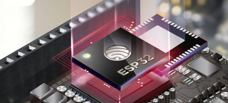
ESP32 is an RISC-based microcontroller widely used among most electronic enthusiasts with the Arduino platform. Since Arduino makes development faster and easier, the boot process of this microcontroller is not widely known among them. So today I will go through what will happen when the power is supplied to the ESP32.
Reset Causes
Every power on, ESP32 looks for the reset cause, depending on the reset cause the flow is different. ESP32 has three different approaches depending on the reset cause.
Reset from a deep sleep:
Software CPU reset, WDT CPU reset
Power on reset, Software SoC reset, WDT SoC reset:
In this write-up, we ignore the first and second cases. These special scenarios will be discussed in another blog very soon and this blog will discuss the third case in deep.
Reset Vector and First Stage Bootloader
Before starting, we should understand that the microcontroller is hard-wired to load a predefined program memory address to the PC when it is started it’s first action, we usually name it a reset vector. In ESP32 this reset vector points to the internal ROM(1) which is programmed by the manufacturer and is read-only. This is also firmware, but it is specific because of a couple of reasons,
The size of the ROM code is very small compared to the application
Only initialize the necessary peripherals that are needed to start the application.
Read-only memory
The firmware inside the ROM is known as, ROM Code, ROM Bootloader, or 1st Stage Bootloader. Please note that sometimes, if this firmware is mentioned as a ROM bootloader, the 1st stage bootloader could be the next application (next firmware) to which the ROM bootloader passes the control. We will discuss this type of boot process in another write-up soon.
In this case, We refer to the first firmware that executes when powered on, and stored in ROM as the 1st bootloader as ESP32 documentation has referred to.
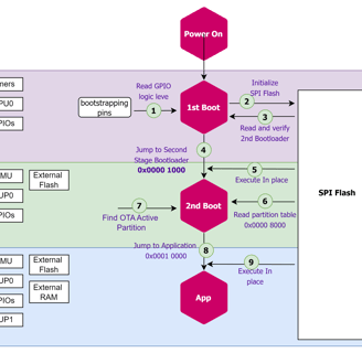
This is the high-level flow of the boot process in ESP32

Let’s dig deeper into each section.
Address space and memory layout
The boot process is tightly coupled with its address space and the memory layout, so understanding the boot process will never be a success without looking into this.
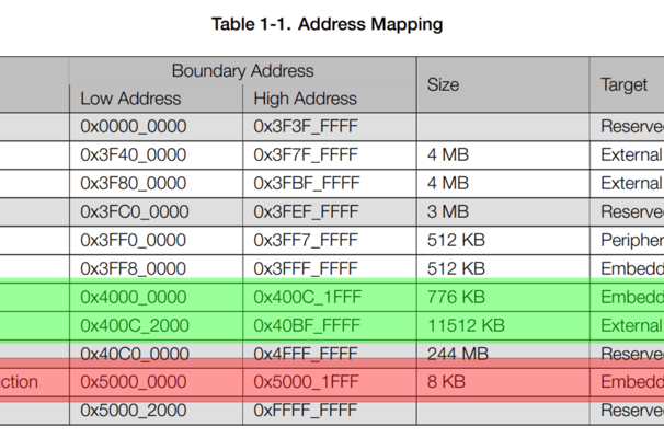
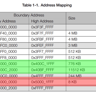
Highlighted in green are used for the boot process that we are discussing today. Highlighted in red is used for a specific feature in ESP32, which is not used and discussed in this write-up.
Boot Stage 1
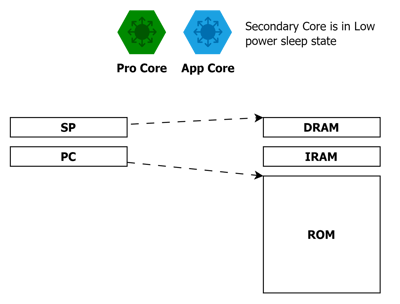
In this stage, the device starts and does the necessary logic depending on the ROM firmware and passes the control to the 2nd Bootloader. During the power on, the device is in the below state, the PC is pointing to ROM and the SP is pointing to DRAM of the ESP32.
Depending on the microcontroller, the duties and responsibilities of the ROM firmware differ slightly.
When the device is powered on, All the initial processing is done by the PRO Core, and the App Core stays in low-power sleep mode. As I mentioned earlier, the ESP32 is hardwired to load instructions from a specific memory address, so during the power-on, the address is loaded to the PC and starts to execute the ROM firmware. In ESP32 the reset vector is 0x40000400
Bootstrapping
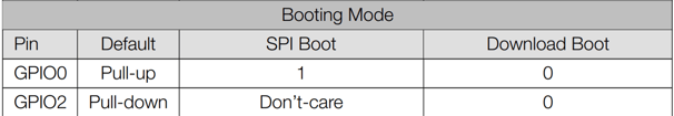
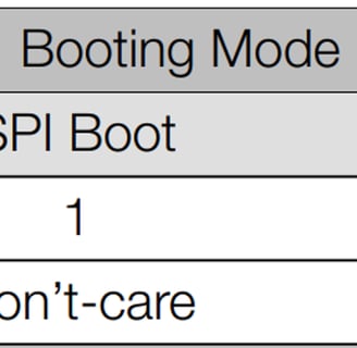
The ROM firmware reads the bootstrapping pins of the ESP32, and through these GPIOs user can pass some information to the ROM firmware. ESP32 has two boot modes,
SPI Boot
Download Boot
Depending on the state of the GPIO0 and GPIO2, the boot mode is selected. As you know, in most of the ESP32 devkits you have seen the “Boot” Button and the reset button, to boot into download mode, you need to press the “Boot” button while you reset the ESP32.
Other than selecting the boot mode, there are a few other configurations that can be done through these strapping pins.
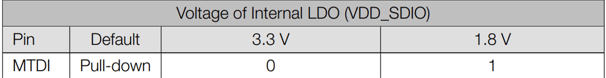
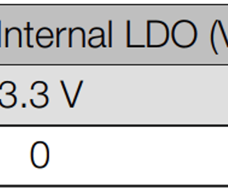
Controlling the output of the internal voltage regulator The voltage of this internal regulator should be configured to match the SPI flash. If you are using the ESP32 module, this is already taken care of.
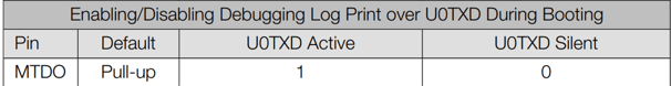
Enable, debug logs to be sent to the UART0TX pin If the debug logs are needed, those can be enabled through this configuration
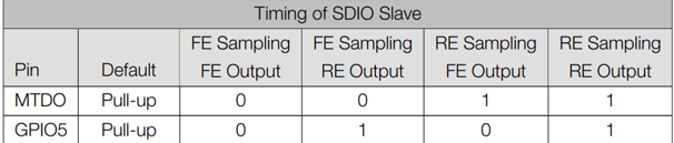
*FE - Falling Edge, RE - Rising Edge
Timing of the SDIO slave This changes the flash interface clock and clock edges. If you are using the ESP32 module, this is already taken care of.
Verify 2nd Stage bootloader
Since the first stage bootloader is manufacturer-fitted and not modifiable, it expects the 1at stage bootloader at SPI flash address 0x0000 1000. If the secure boot is enabled, it will utilize the first 4K bytes. In this, we are not looking for a secure boot option. So the first 4KB is ignored.
1st stage bootloader verifies the details of the 2nd stage bootloader by the details encoded in the image header. The below diagram shows an example address map of the 4MB SPI flash with OTA support.
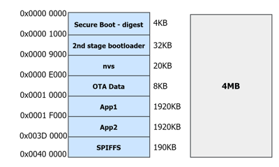
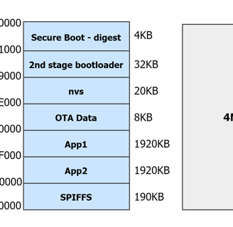
Once the bootloader is verified, 1st stage bootloader jumps to 2nd stage bootloader.
Boot Stage 2: 2nd Bootloader
In this stage, 2nd bootloader starts with its duties and passes the control over to the application. The 2nd stage bootloader is open-source firmware, user can customize as per requirement. However, the default second-stage bootloader shipped with ESP-IDF is a powerful bootloader with many features including OTA support.
I will be explaining the default bootloader shipped with ESP-IDF, and depending on your requirement you can customize it by modifying the bootloader source code. The customization to the default bootloader is out of the scope of this document and we will bring an article on “Adding and removing features to ESP32 2nd stage bootloader” soon. From here onwards, I am referring to the default bootloader shipped with ESP32 with minimum features enabled.
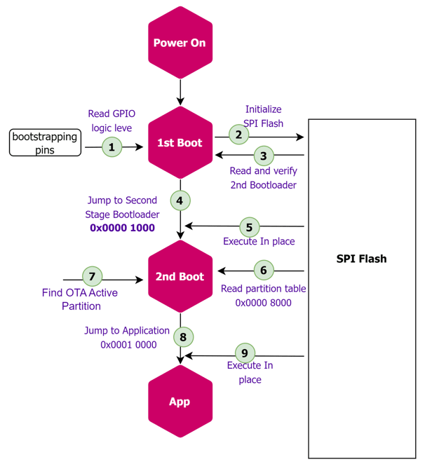
Reading partition table
Once the bootloader gets the control, it is looking for the partition table. Reads the partition table. If the OTA section is available in the table, then ESP32 checks which partition should be used for the next boot cycle.
Identify OTA and next boot section
ESP32 uses an A/B partition scheme to support OTA, which means ESP32 has two partitions that have similar and sufficient capacity to store the firmware. The new firmware will be always updated to the other section of the memory. Ex, if A is currently used, B will be used to write the new firmware.
Memory loading and configurations
Identified binary images will be used to update the memory layout accordingly and configure the MMU for both PRO and APP cores. Finally, validate the application and pass the control to the application.
Boot Stage 3: Application startup
The second stage bootloader will be calling the nonreturnable startup function pointer to pass the control to the application, depending on the architecture of the application the process of the initialization and setting up the ESP32 to run the application logic and the peripherals is different. The ESP32 follows an organized way of this, which also be converted to a write-up soon.
Once the configuration is done, additional CUPs will be started as well.
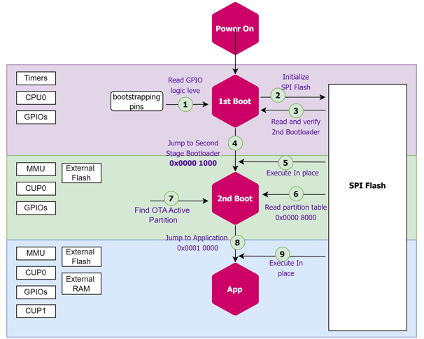
Peripheral usage during each stage of the boot process.
Notes
(1) - If the RTC slow or fast memories have been used to optimize the boot time through the STAT_VECTOR_SEL registers, the device starts from the RTC memory but not ROM.